- 您现在的位置:买卖IC网 > Sheet目录2011 > MAX5877EGK+D (Maxim Integrated Products)IC DAC 14BIT DUAL 250MSPS 68-QFN
MAX5877
14-Bit, 250Msps, High-Dynamic-Performance,
Dual DAC with LVDS Inputs
14
______________________________________________________________________________________
CMOS-Compatible Digital Inputs
Input Data Format Select (TORB)
The TORB input selects between two’s-complement or
offset binary digital input data. Set TORB to a CMOS-
logic-high level to indicate a two’s-complement input
format. Set TORB to a CMOS-logic-low level to indicate
an offset binary input format.
Power-Down Operation (PD)
The MAX5877 also features an active-high power-down
mode that reduces the DAC’s digital current consump-
tion from 34mA to less than 5A and the analog current
consumption from 82mA to less than 2A. Set PD high
to power down the MAX5877. Set PD low for normal
operation.
When powered down, the MAX5877 reduces the overall
power consumption to less than 16W. The MAX5877
requires 10ms to wake up from power-down and enter
a fully operational state. The PD integrated pulldown
resistor activates the MAX5877 if PD is left floating.
Applications Information
CLK Interface
The MAX5877 features a flexible differential clock input
(CLKP, CLKN) with a separate supply (AVCLK) to
achieve optimum jitter performance. Use an ultra-low
jitter clock to achieve the required noise density. Clock
jitter must be less than 0.5psRMS for meeting the speci-
fied noise density. For that reason, the CLKP/CLKN
input source must be designed carefully. The differen-
tial clock (CLKN and CLKP) input can be driven from a
single-ended or a differential clock source. Differential
clock drive is required to achieve the best dynamic
performance from the DAC. For single-ended opera-
tion, drive CLKP with a low noise source and bypass
CLKN to GND with a 0.1F capacitor.
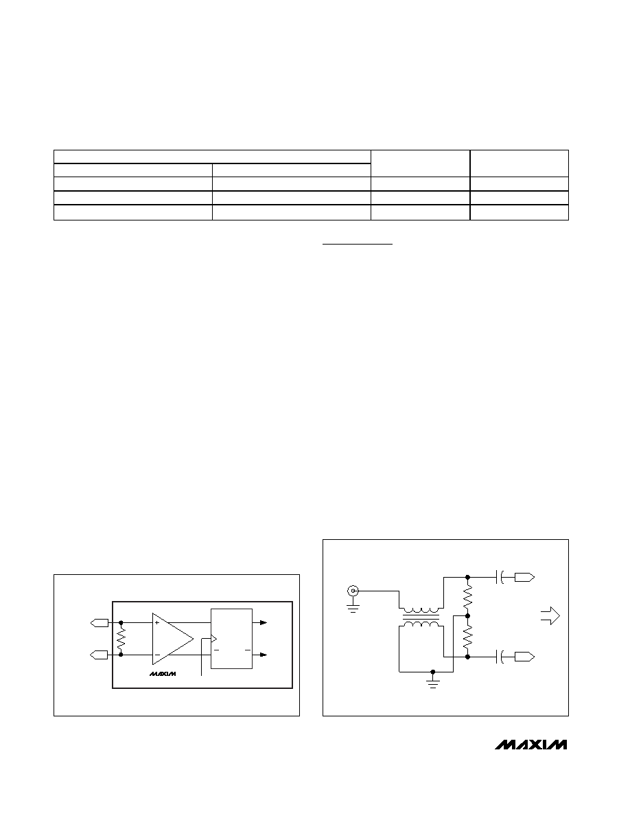
Figure 6 shows a convenient and quick way to apply a
differential signal created from a single-ended source
(e.g., HP 8662A signal generator) and a wideband trans-
former. Alternatively, these inputs can be driven from a
CMOS-compatible clock source; however, it is recom-
mended to use sinewave or AC-coupled differential
ECL/PECL or LVDS drive for best dynamic performance.
110
TO
DECODE
LOGIC
D
Q
B13P–B0P,
SELIQP
B13N–B0N,
SELIQN
CLOCK
MAX5877
Figure 5. Simplified LVDS-Compatible Digital Input Structure
DIGITAL INPUT CODE
OFFSET BINARY
TWO’S COMPLEMENT
OUT_P
OUT_N
00 0000 0000 0000
10 0000 0000 0000
0
IOUTFS
01 1111 1111 1111
00 0000 0000 0000
IOUTFS / 2
11 1111 1111 1111
01 1111 1111 1111
IOUTFS
0
Table 2. DAC Output Code Table
WIDEBAND RF TRANSFORMER
PERFORMS SINGLE-ENDED-TO-
DIFFERENTIAL CONVERSION
SINGLE-ENDED
CLOCK SOURCE
(e.g., HP 8662A)
GND
1:1
25
25
CLKP
CLKN
TO DAC
0.1
F
0.1
F
Figure 6. Differential Clock-Signal Generation
发布紧急采购,3分钟左右您将得到回复。
相关PDF资料
MAX5878EGK+D
IC DAC 16BIT DUAL 250MSPS 68-QFN
MAX5884EGM+D
IC DAC 14BIT 3.3V 200MSPS 48-QFN
MAX5885EGM+D
IC DAC 16BIT 3.3V 200MSPS 48-QFN
MAX5886EGK+D
IC DAC 12BIT 3.3V 500MSPS 68-QFN
MAX5887EGK+D
IC DAC 14BIT 3.3V 500MSPS 68-QFN
MAX5888EGK+D
IC DAC 16BIT 3.3V 500MSPS 68-QFN
MAX5889EGK+D
IC DAC 12BIT LVDS 600MSPS 68-QFN
MAX5890EGK+D
IC DAC 14BIT LVDS 600MSPS 68-QFN
相关代理商/技术参数
MAX5877EGK+TD
功能描述:数模转换器- DAC 14-Bit 2Ch 250Msps DAC RoHS:否 制造商:Texas Instruments 转换器数量:1 DAC 输出端数量:1 转换速率:2 MSPs 分辨率:16 bit 接口类型:QSPI, SPI, Serial (3-Wire, Microwire) 稳定时间:1 us 最大工作温度:+ 85 C 安装风格:SMD/SMT 封装 / 箱体:SOIC-14 封装:Tube
MAX5877EGK-D
功能描述:数模转换器- DAC RoHS:否 制造商:Texas Instruments 转换器数量:1 DAC 输出端数量:1 转换速率:2 MSPs 分辨率:16 bit 接口类型:QSPI, SPI, Serial (3-Wire, Microwire) 稳定时间:1 us 最大工作温度:+ 85 C 安装风格:SMD/SMT 封装 / 箱体:SOIC-14 封装:Tube
MAX5877EGK-TD
功能描述:数模转换器- DAC RoHS:否 制造商:Texas Instruments 转换器数量:1 DAC 输出端数量:1 转换速率:2 MSPs 分辨率:16 bit 接口类型:QSPI, SPI, Serial (3-Wire, Microwire) 稳定时间:1 us 最大工作温度:+ 85 C 安装风格:SMD/SMT 封装 / 箱体:SOIC-14 封装:Tube
MAX5877EVKIT#
功能描述:数模转换器- DAC Evaluation Kit for the MAX5876/MAX5877/MAX5878 RoHS:否 制造商:Texas Instruments 转换器数量:1 DAC 输出端数量:1 转换速率:2 MSPs 分辨率:16 bit 接口类型:QSPI, SPI, Serial (3-Wire, Microwire) 稳定时间:1 us 最大工作温度:+ 85 C 安装风格:SMD/SMT 封装 / 箱体:SOIC-14 封装:Tube
MAX5878EGK
制造商:Rochester Electronics LLC 功能描述: 制造商:Maxim Integrated Products 功能描述:
MAX5878EGK+D
功能描述:数模转换器- DAC 16-Bit 2Ch 250Msps DAC RoHS:否 制造商:Texas Instruments 转换器数量:1 DAC 输出端数量:1 转换速率:2 MSPs 分辨率:16 bit 接口类型:QSPI, SPI, Serial (3-Wire, Microwire) 稳定时间:1 us 最大工作温度:+ 85 C 安装风格:SMD/SMT 封装 / 箱体:SOIC-14 封装:Tube
MAX5878EGK+TD
功能描述:数模转换器- DAC 16-Bit 2Ch 250Msps DAC RoHS:否 制造商:Texas Instruments 转换器数量:1 DAC 输出端数量:1 转换速率:2 MSPs 分辨率:16 bit 接口类型:QSPI, SPI, Serial (3-Wire, Microwire) 稳定时间:1 us 最大工作温度:+ 85 C 安装风格:SMD/SMT 封装 / 箱体:SOIC-14 封装:Tube
MAX5878EGK-D
功能描述:数模转换器- DAC RoHS:否 制造商:Texas Instruments 转换器数量:1 DAC 输出端数量:1 转换速率:2 MSPs 分辨率:16 bit 接口类型:QSPI, SPI, Serial (3-Wire, Microwire) 稳定时间:1 us 最大工作温度:+ 85 C 安装风格:SMD/SMT 封装 / 箱体:SOIC-14 封装:Tube